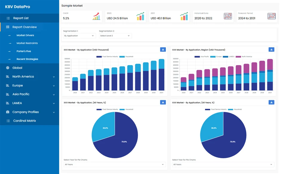
The Global Semiconductor Bonding Market size is expected to reach $1.1 billion by 2030, rising at a market growth of 3.6% CAGR during the forecast period.
With the preferred image quality, CMOS image sensors have produced much speedier inspection systems. Therefore, CMOS Image Sensors would generate approximately 16% share of the market by 2030. For machine vision applications, the designers of CMOS imaging technology are also delivering products with exceptional performance. CMOS image sensors are commonly used in camera-enabled mobile phones due to their smaller size, lower power consumption, and greater speed than CCD image sensors. Social networking's growing popularity has increased consumer demand for high-end camera features in mobile phones, driving up demand for CMOS image sensors. Some of the factors impacting the market are growing stacked die technology adoption for IoT devices, expansion of microelectronics’ demand, and a substantial cost of ownership.
![]()
This market is expanding as stacked die technology is increasingly used in IoT devices. Typically, bare dies are stacked one on top of the other inside a single semiconductor package to utilize the same placement area on a substrate for several functionalities. The electrical performance of devices is improved by die stacking because faster signal production is achieved through shorter routing of interconnections between circuits. IoT devices compactly bond several stacked dies to substrates using semiconductor bonding processes. Therefore, considering this growing IoT devices usage of stacked die technology, the market is expected to grow. Additionally, the market will expand more quickly due to the growing interest in electric vehicles and micro-electromechanical systems. The rapid rise of the market will be aided by introducing the 5G network and increasing research into developing the 6G network. Wearable technology and smartphone usage will grow, influencing market trends. Strong connections between these stacked layers are formed using semiconductor bonding techniques. As a result of the rising microelectronics demand, the market is expected to grow.
However, Die-attach operations require sophisticated machinery that requires a substantial amount of input power. Hundreds to thousands of watts are consumed by these pieces of equipment. Due to intricate and expensive components, semiconductor bonding equipment has a very high manufacturing cost. The assembly of various large and small parts, including the display, bonding hand, vacuum, sensors, and heat source, is also expensive. Since most of the equipment involved in semiconductor bonding is expensive, it restricts market entry for many businesses, which in turn results in slower market growth.
By type, the market is categorized into die bonder, wafer bonder, and flip chip bonder. The wafer bonder segment held the highest revenue share in the market in 2022. Wafer bonding is increasingly used in silicon-on-insulator (SOI) devices, silicon-based sensors and actuators, and optical devices. Wafer bonding technology offers several advantages, including the ability to bond diverse compounds, prevent surface bubbles, bond at low temperatures and under high vacuum, and thin wafers for smart cut procedures. Wafer bonding permits some design and production flexibility in terms of material combination, which undoubtedly contributes significantly to the expansion of the market.
![]()
By application, the market is divided into RF devices, Mems and sensors, CMOS image sensors, LED, and 3D NAND. In 2022, the Mems and sensors segment projected a prominent revenue share in the market. Semiconductor bonding has numerous applications in micro-electromechanical systems (MEMS), sensors, integrated circuits, power electronics, and micro/nanofluidics. The MEMS and sensors segment is anticipated to rise due to the increasing use of wafer-bonding technology in creating MEMS, optoelectronics, sensors, and high-power electronics.
On the basis of bonding technology, the market is divided into die bonding technology and wafer bonding technology. In 2022, the wafer bonding technology segment garnered a significant revenue share in the market in 2022. Due to the growing demand for stable joining and bonding of two substrates in industrial applications, there is a significant demand for wafer bonders. One of the quickest methods for producing several III-V lasers on Si material in a parallel system is wafer bonding. A key cause creating new prospects for market vendors for semiconductor bonding applications is the rising demand for consumer electronic devices like smartphones, smart wearables, smart lighting, and other RF devices.
Based on process type, the market is classified into die-to-die bonding, die to wafer bonding, and wafer to wafer bonding. The die-to-die bonding segment witnessed the largest revenue share in the market in 2022. Die-to-die bonding involves stacking, bonding, and packaging each die separately to create a stacked die. To provide an evanescent optical connection between III-V layers and silicon waveguides by developing a die-to-die adhesive bonding process that produces thick bonding layers less than 100 nm.
| Report Attribute | Details |
|---|---|
| Market size value in 2022 | USD 865.5 Million |
| Market size forecast in 2030 | USD 1.1 Billion |
| Base Year | 2022 |
| Historical Period | 2019 to 2021 |
| Forecast Period | 2023 to 2030 |
| Revenue Growth Rate | CAGR of 3.6% from 2023 to 2030 |
| Number of Pages | 353 |
| Number of Table | 530 |
| Report coverage | Market Trends, Revenue Estimation and Forecast, Segmentation Analysis, Regional and Country Breakdown, Companies Strategic Developments, Company Profiling |
| Segments covered | Type, Bonding Technology, Process Type, Application, Region |
| Country scope | US, Canada, Mexico, Germany, UK, France, Russia, Spain, Italy, China, Japan, India, South Korea, Singapore, Malaysia, Brazil, Argentina, UAE, Saudi Arabia, South Africa, Nigeria |
| Growth Drivers |
|
| Restraints |
|
Region wise, the market is analysed across North America, Europe, Asia Pacific, and LAMEA. In 2022, the Asia Pacific region led the market by generating the highest revenue share. Due to the region's well-established semiconductor sector, a major player in the market, and strategic investments made by significant domestic suppliers. The region is home to some of the world's largest semiconductor companies, and growing investments are being made in China, India, and Vietnam to support the semiconductor industry's infrastructure. In addition, reputable domestic vendors and government agencies are investing significantly in technology to offer future semiconductor bonding solutions, such as hybrid bonding, which is expected to increase market demand.
The market research report covers the analysis of key stake holders of the market. Key companies profiled in the report include Mycronic AB, TDK Corporation, EV Group, Panasonic Holdings Corporation, Tokyo Electron Ltd., Mitsubishi Electric Corporation, Intel Corporation, SÜSS MicroTec SE, Fuji Corporation (Fasford Technology Co., Ltd.), Shibuara Mechatronics Corporation
Free Valuable Insights: Global Semiconductor Bonding Market size to reach USD 1.1 Billion by 2030
By Application
By Type
By Bonding Technology
By Process Type
By Geography


The Market size is projected to reach USD 1.1 billion by 2030.
Mycronic AB, TDK Corporation, EV Group, Panasonic Holdings Corporation, Tokyo Electron Ltd., Mitsubishi Electric Corporation, Intel Corporation, S�SS MicroTec SE, Fuji Corporation (Fasford Technology Co., Ltd.), Shibuara Mechatronics Corporation
Mycronic AB, TDK Corporation, EV Group, Panasonic Holdings Corporation, Tokyo Electron Ltd., Mitsubishi Electric Corporation, Intel Corporation, SÜSS MicroTec SE, Fuji Corporation (Fasford Technology Co., Ltd.), Shibuara Mechatronics Corporation
The Die Bonding Technology segment acquired maximum revenue share in the Market by Bonding Technology in 2022; thereby, achieving a market value of $708.2 million by 2030.
The LED segment is leading the Market by Application in 2022; thereby, achieving a market value of $411.7 million by 2030.
The North America region dominated the Market by Region in 2022 and would continue to be a dominant market till 2030; thereby, achieving a market value of $308.2 million by 2030.
Our team of dedicated experts can provide you with attractive expansion opportunities for your business.
