The Europe Semiconductor Bonding Market would witness market growth of 3.4% CAGR during the forecast period (2023-2030).
A flip-chip bonder is commonly referred to as a controlled collapse chip connection. It is also referred to briefly as C4. This equipment aims to connect dies to one another. Semiconductor devices, passive integrated devices, and IC chips are some of the dies. Solder bumps are used to attach these dies to external circuitry. The utilization of flip-chip bonders is becoming more and more needed as smart manufacturing, smart factories, and smart grids emerge. In addition, they are utilized within the architecture of microelectromechanical system sensors. Flip chip bonding helps to eliminate the use of wire bonds. These elements collectively significantly contribute to the market growth.
Flip chip bonders are beneficial for miniaturizing sensors. This is a crucial element that is fueling their demand. Flip chip bonds can also be utilized as packaging materials for electronic items. Infrared sensors, integrated circuits, optical components, surface acoustic wave (or SAW) devices, and detector arrays are examples of electronic items. The electronic sector has a considerable demand for these bonds. This can have a positive effect on the growth of the market.
In 2016, Spain introduced the industrial digitalization initiative Connected Industry 4.0, which aimed to offer a digital transformation strategy for companies. The initiative's key goals include boosting the sector's industrial-added value and qualified employment while preferring the Spanish model for emerging sectors and the local supply of digital solutions. The context and action fields for deploying 5G networks in Germany by 2025 are described in the Federal Government's 5G Strategy. As a result of such developments, Europe’s regional market will witness significant growth throughout the forecast period.
The Germany market dominated the Europe Semiconductor Bonding Market by Country in 2022 and would continue to be a dominant market till 2030; thereby, achieving a market value of $66.2 million by 2030. The UK market is estimated to grow at a CAGR of 2.5% during (2023 - 2030). Additionally, The France market would register a CAGR of 4.2% during (2023 - 2030).
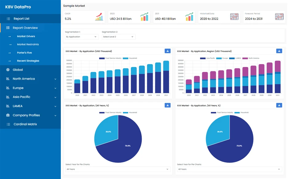
Based on Application, the market is segmented into LED, Mems & Sensors, RF Devices, CMOS Image Sensors, and 3D NAND. Based on Type, the market is segmented into Wafer Bonder, Die Bonder, and Flip Chip Bonder. Based on Bonding Technology, the market is segmented into Die Bonding Technology, and Wafer Bonding Technology (Direct & Anodic Wafer Bonding, and Indirect Wafer Bonding). Based on Process Type, the market is segmented into Die To Die Bonding, Wafer To Wafer Bonding, and Die To Wafer Bonding. Based on countries, the market is segmented into Germany, UK, France, Russia, Spain, Italy, and Rest of Europe.
Free Valuable Insights: The Worldwide Semiconductor Bonding Market is Projected to reach USD 1.1 Billion by 2030, at a CAGR of 3.6%
The market research report covers the analysis of key stakeholders of the market. Key companies profiled in the report include Mycronic AB, TDK Corporation, EV Group, Panasonic Holdings Corporation, Tokyo Electron Ltd., Mitsubishi Electric Corporation, Intel Corporation, SÜSS MicroTec SE, Fuji Corporation (Fasford Technology Co., Ltd.), Shibuara Mechatronics Corporation
By Application
By Type
By Bonding Technology
By Process Type
By Country
Our team of dedicated experts can provide you with attractive expansion opportunities for your business.