The North America Semiconductor Metrology and Inspection Equipment Market is expected to reach USD 6.0 billion by 2032, growing at a CAGR of 6.9% during (2026 – 2033).
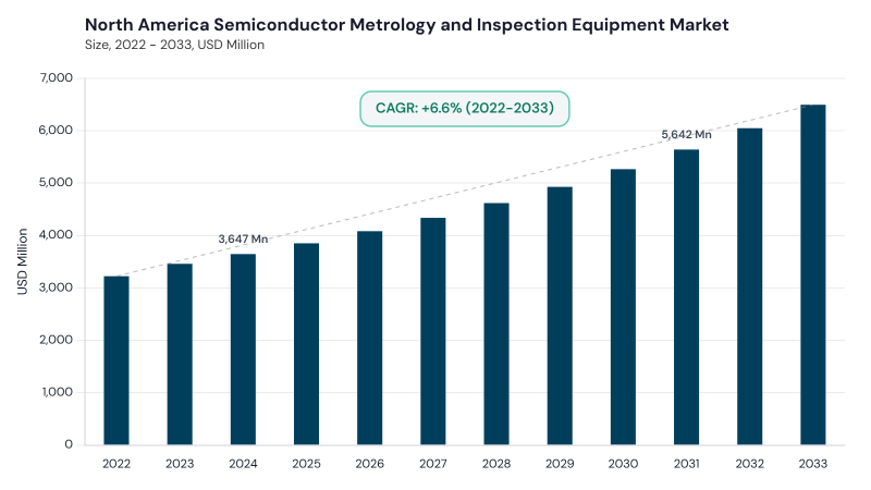
The North America Semiconductor Metrology and Inspection Equipment Market developed from the semiconductor industry’s growing need for precise measurement, wafer verification, and defect detection. Early inspection practices relied on manual methods, optical tools, and basic dimensional checks to support wafer and component quality control. As lithography improved and device geometries became smaller, the market shifted toward non-contact optical metrology, electron beam inspection, scatterometry, ellipsometry, and critical dimension measurement. The rise of advanced nodes, multilayer devices, and complex chip architectures increased the need for automated, high-resolution, and inline inspection systems.
The North America Semiconductor Metrology and Inspection Equipment Market is being shaped by semiconductor miniaturization, advanced lithography, heterogeneous integration, regional fab expansion, and stricter quality requirements. Manufacturers are using metrology and inspection systems to detect nanoscale defects, monitor wafer quality, improve process repeatability, and reduce production losses. Demand is supported by government-backed semiconductor investments, onshore manufacturing capacity, advanced packaging development, and rising need for high-performance chips. Vendors are focusing on AI-based defect classification, high-throughput inspection, inline metrology, automation-ready platforms, and software-driven analytics.
Based on Type, the market is segmented into Optical and Beam. The Optical market dominated the North America Semiconductor Metrology and Inspection Equipment Market by Type in 2025, and would continue to be a dominant market till 2033; thereby, achieving a market value of USD 4.2 billion by 2032, growing at a CAGR of 6.5 % during the forecast period. The Beam market is expected to witness a CAGR of 7.7% during (2026 - 2033).
Optical leads due to its high-speed, non-contact inspection capability, strong suitability for inline wafer monitoring, and broad use in high-volume semiconductor manufacturing. Optical systems support defect detection, film measurement, overlay control, critical dimension analysis, and surface inspection while maintaining production throughput. Demand is reinforced by smaller process nodes, advanced chip architectures, and the need for fast, reliable inspection across fabrication lines. Beam-based systems remain important for nanoscale defect review, high-resolution imaging, EUV-related process control, and advanced logic and memory applications where optical tools may face resolution limitations.
Based on Dimension, the market is segmented into 2D Metrology/Inspection, 3D Metrology/Inspection, and Hybrid 2D/3D Systems. The 2D Metrology/Inspection market dominated the North America Semiconductor Metrology and Inspection Equipment Market by Dimension in 2025, and would continue to be a dominant market till 2033; thereby, achieving a market value of USD 2.7 billion by 2032, growing at a CAGR of 6.4 % during the forecast period. The 3D Metrology/Inspection market is expected to witness a CAGR of 7.2% during (2026 - 2033). The Hybrid 2D/3D Systems market is expected to witness a CAGR of 7.2% during (2026 - 2033).
2D Metrology/Inspection leads due to its extensive use in planar wafer inspection, lithography verification, overlay measurement, line-width control, and routine defect monitoring. These systems remain essential across semiconductor fabs because they offer speed, reliability, and cost-effective inline process support. 3D Metrology/Inspection is gaining traction as manufacturers adopt FinFET structures, 3D NAND, stacked dies, through-silicon vias, and advanced packaging formats that require volumetric inspection. Hybrid 2D/3D Systems are expanding as fabs seek integrated platforms that combine planar and structural analysis to improve process control, reduce tool footprint, and support increasingly complex device geometries.
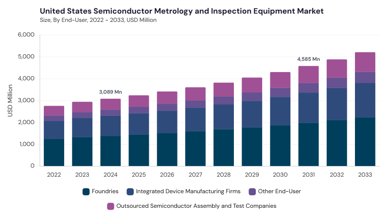
Based on End-User, the market is segmented into Foundries, Integrated Device Manufacturing Firms, Outsourced Semiconductor Assembly and Test Companies, and Other End-User. The Foundries market dominated the North America Semiconductor Metrology and Inspection Equipment Market by End-User in 2025, and would continue to be a dominant market till 2033; thereby, achieving a market value of USD 2.6 billion by 2032, growing at a CAGR of 6.3 % during the forecast period. The Integrated Device Manufacturing Firms market is expected to witness a CAGR of 7% during (2026 - 2033). Additionally, The Outsourced Semiconductor Assembly and Test Companies market is expected to witness highest CAGR of 7.7% during (2026 - 2033).
Foundries lead due to their strong dependence on advanced metrology and inspection systems for yield improvement, process stability, customer specification compliance, and high-volume wafer fabrication. These facilities require precise tools for defect detection, overlay alignment, critical dimension measurement, and inline quality control across multiple technology nodes. Integrated Device Manufacturing Firms use metrology equipment for process development, prototyping, production validation, and package-level quality assurance. Outsourced Semiconductor Assembly and Test Companies and Other End-User areas add demand through advanced packaging inspection, wire bond analysis, solder joint evaluation, failure analysis, materials research, specialty semiconductor development, and academic process innovation.
Based on Technology, the market is segmented into Wafer Inspection System, Thin Film Metrology, Mask Inspection System, Package Inspection, and Other Technology. Wafer Inspection System leads due to its critical role in early defect detection, wafer quality control, process monitoring, and yield enhancement across semiconductor fabrication. These systems help identify contamination, pattern defects, process variation, and fabrication anomalies before they affect downstream production.
Thin Film Metrology supports accurate measurement of deposited layers, refractive properties, film thickness, and uniformity across front-end and back-end manufacturing steps. Mask Inspection System, Package Inspection, and Other Technology areas add demand through photomask defect detection, package reliability checks, advanced X-ray inspection, electrical metrology, atomic force microscopy, material characterization, and specialized process development.
Free Valuable Insights: The Global Semiconductor Metrology and Inspection Equipment Market will hit USD 26.8 Billion billion by 2033, at a CAGR of 7.6%
Based on Country, the market is segmented into US, Canada, Mexico, and Rest of North America. The US market dominated the North America Semiconductor Metrology and Inspection Equipment Market by Country in 2025, and would continue to be a dominant market till 2033; thereby, achieving a market value of USD 4.9 billion by 2032, growing at a CAGR of 6.2 % during the forecast period. The Canada market is expected to witness a CAGR of 10.2% during (2026 - 2033). Additionally, The Mexico market is expected to witness a CAGR of 8.6% during (2026 - 2033).
The US leads due to strong semiconductor manufacturing investments, advanced fab development, domestic supply chain initiatives, AI-driven inspection adoption, and demand for high-precision tools supporting advanced nodes and packaging technologies. Canada supports market growth through hybrid metrology adoption, research-led semiconductor innovation, machine learning-based process control, and growing focus on domestic inspection capabilities. Mexico is advancing through semiconductor manufacturing expansion, 3D chip inspection demand, AI-enabled quality control, and localized equipment support for emerging fabrication and assembly operations. Rest of North America benefits from advanced packaging activity, AI-assisted analytics, regional support networks, sustainability-focused equipment design, and broader adoption of automated metrology systems.
By Type
By Dimension
By End-User
By Technology
By Country
Set to reach $6.0 Billion by 2032, growing at 6.9% CAGR during 2026-2033.
The US leads with $4.9 billion by 2032, growing at 6.2% CAGR during the forecast period.
Rising demand for advanced metrology in semiconductor manufacturing fuels market growth.
The optical segment will reach $4.2 billion by 2032, growing at 6.5% CAGR during the forecast period.
The Canada market is expected to witness a CAGR of 10.2% during 2026-2033.
The 2D metrology/inspection segment will reach $2.7 billion by 2032, growing at 6.4% CAGR during the forecast period.
Our team of dedicated experts can provide you with attractive expansion opportunities for your business.




 Unique Offerings