The sample copy of this report is available for access.
The LAMEA Semiconductor Metrology and Inspection Equipment Market is expected to reach USD 1.2 billion by 2029, growing at a CAGR of 9.3% during (2026 – 2033).
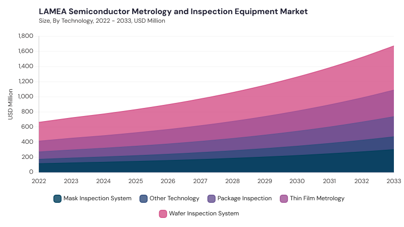
The LAMEA Semiconductor Metrology and Inspection Equipment Market developed from early semiconductor quality-control practices focused on basic dimensional checks and visual wafer inspection. Initial adoption was limited to simple optical tools and manual verification methods used to reduce fabrication errors and improve yield. Over time, rising device complexity encouraged the adoption of optical, electron-beam, atomic force microscopy, scattering, and X-ray-based inspection technologies. The shift from larger wafer formats to automated, high-precision fabrication increased the need for inline monitoring and integrated metrology platforms.
The LAMEA Semiconductor Metrology and Inspection Equipment Market is being shaped by semiconductor manufacturing expansion, advanced device structures, quality-control pressure, specialty semiconductor demand, and regional supply-chain localization. Manufacturers are using metrology and inspection systems to improve wafer yield, verify thin films, detect defects earlier, monitor masks, and strengthen package reliability. Demand is supported by increasing activity in automotive electronics, telecommunications, industrial devices, IoT infrastructure, renewable energy systems, and localized semiconductor initiatives. Vendors are focusing on machine learning-enabled inspection, modular platforms, inline metrology, non-destructive testing, regional service networks, and customized solutions suited to varied infrastructure conditions.
Based on Type, the market is segmented into Optical and Beam. The Optical market dominated the LAMEA Semiconductor Metrology and Inspection Equipment Market by Type in 2025, and would continue to be a dominant market till 2033; thereby, achieving a market value of USD 819.3 million by 2029, growing at a CAGR of 8.9 % during the forecast period. The Beam market is expected to witness a CAGR of 10.3% during (2026 - 2033).
Optical leads due to its high-throughput, non-contact measurement capability, suitability for inline inspection, and cost-effective use across wafer monitoring and production quality control. These systems support film thickness measurement, surface inspection, overlay control, lithographic pattern verification, and defect identification across different semiconductor fabrication steps. Demand is supported by regional investment in manufacturing capabilities and the need for reliable inspection tools that balance speed with measurement repeatability. Beam-based systems remain important for high-resolution defect analysis, photomask inspection, failure analysis, and advanced-node applications where sub-nanometer sensitivity and deeper defect characterization are required.
Based on Dimension, the market is segmented into 2D Metrology/Inspection, 3D Metrology/Inspection, and Hybrid 2D/3D Systems. The 2D Metrology/Inspection market dominated the LAMEA Semiconductor Metrology and Inspection Equipment Market by Dimension in 2025, and would continue to be a dominant market till 2033; thereby, achieving a market value of USD 539.5 million by 2029, growing at a CAGR of 8.9 % during the forecast period. The 3D Metrology/Inspection market is expected to witness a CAGR of 9.7% during (2026 - 2033). The Hybrid 2D/3D Systems market is expected to witness a CAGR of 9.8% during (2026 - 2033).
2D Metrology/Inspection leads due to its established use in planar wafer inspection, linewidth measurement, overlay verification, dimensional control, and routine defect monitoring. These systems remain preferred across LAMEA because they offer operational efficiency, lower complexity, and strong suitability for mature-node and cost-sensitive manufacturing environments. 3D Metrology/Inspection is gaining demand as manufacturers adopt advanced packaging, stacked devices, FinFET structures, TSVs, and multilayer semiconductor architectures. Hybrid 2D/3D Systems are gradually expanding as fabs seek integrated platforms that combine surface and volumetric analysis to improve defect detection, reduce tool duplication, and support broader process optimization.
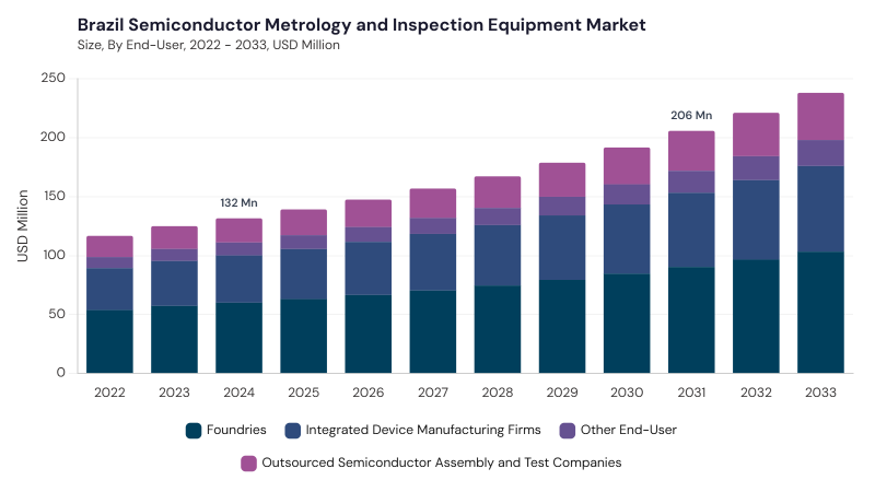
Based on End-User, the market is segmented into Foundries, Integrated Device Manufacturing Firms, Outsourced Semiconductor Assembly and Test Companies, and Other End-User. The Foundries market dominated the LAMEA Semiconductor Metrology and Inspection Equipment Market by End-User in 2025, and would continue to be a dominant market till 2033; thereby, achieving a market value of USD 515.8 million by 2029, growing at a CAGR of 8.7 % during the forecast period. The Integrated Device Manufacturing Firms market is expected to witness a CAGR of 9.5% during (2026 - 2033). Additionally, The Outsourced Semiconductor Assembly and Test Companies market is expected to witness highest CAGR of 10.2% during (2026 - 2033).
Foundries lead due to their strong requirement for process control, defect minimization, wafer-level inspection, and yield improvement across fabrication operations. These facilities use metrology tools for critical dimension measurement, overlay alignment, thin film monitoring, and inline feedback as regional semiconductor capabilities develop. Integrated Device Manufacturing Firms deploy inspection equipment across design, fabrication, assembly, and testing workflows to improve product quality and operational consistency. Outsourced Semiconductor Assembly and Test Companies and Other End-User areas add demand through package inspection, solder joint evaluation, wire bond verification, research activity, prototype development, specialty semiconductor production, and localized innovation programs.
Based on Technology, the market is segmented into Wafer Inspection System, Thin Film Metrology, Mask Inspection System, Package Inspection, and Other Technology. Wafer Inspection System leads due to its central role in detecting particles, pattern defects, process variations, and wafer-level irregularities during fabrication. These systems help manufacturers reduce scrap, improve yield, and maintain process consistency as device structures become more complex.
Thin Film Metrology remains important for monitoring deposition accuracy, film thickness, layer uniformity, refractive properties, and material performance across semiconductor production. Mask Inspection System, Package Inspection, and Other Technology areas add demand through photomask defect detection, package integrity checks, X-ray inspection, automated optical inspection, defect review tools, electrical probe stations, contamination analysis, and specialized failure diagnostics.
Free Valuable Insights: Semiconductor Metrology and Inspection Equipment Market Size Worth USD 26.8 Billion billion by 2033
Based on Country, the market is segmented into Brazil, Argentina, UAE, Saudi Arabia, South Africa, Nigeria, and Rest of LAMEA. The Brazil market dominated the LAMEA Semiconductor Metrology and Inspection Equipment Market by Country in 2025, and would continue to be a dominant market till 2033; thereby, achieving a market value of USD 178.8 million by 2029, growing at a CAGR of 7.1 % during the forecast period. The Argentina market is expected to witness a CAGR of 11.4% during (2026 - 2033). Additionally, The UAE market is expected to witness a CAGR of 8.3% during (2026 - 2033).
Brazil leads due to growing semiconductor fabrication activity, hybrid metrology adoption, inline inspection demand, localized service support, and rising interest in advanced defect detection tools. Argentina supports market growth through academic and industrial semiconductor initiatives, AI-enabled analytics, regional supply-chain localization, and gradual adoption of advanced process control systems. The UAE contributes through semiconductor ecosystem development, hybrid metrology investment, automation-focused inspection, and demand for high-precision tools aligned with localized manufacturing ambitions. Saudi Arabia, South Africa, and Nigeria add momentum through digital industrialization, inspection infrastructure development, service localization, workforce training, and AI-enabled quality-control adoption, while Rest of LAMEA benefits from targeted semiconductor modernization and customized equipment deployment.
By Type
By Dimension
By End-User
By Technology
By Country
Set to reach $1.2 Billion by 2029, growing at 9.3% CAGR during (2026-2033).
Brazil leads with $178.8 million by 2029, growing at 7.1% CAGR during the forecast period.
Optical segment leads with $819.3 million by 2029, growing at 8.9% CAGR during the forecast period.
2D metrology/inspection hits $539.5 million by 2029, growing at 8.9% CAGR during the forecast period.
UAE market is expected to witness a CAGR of 8.3% during (2026-2033).
Expected to witness the highest CAGR of 10.2% during (2026-2033).
Our team of dedicated experts can provide you with attractive expansion opportunities for your business.




 Unique Offerings