The Europe Semiconductor Metrology and Inspection Equipment Market is expected to reach USD 5.5 billion by 2031, growing at a CAGR of 7.4% during (2026 – 2033).
The Europe Semiconductor Metrology and Inspection Equipment Market developed from early optical and electrical inspection tools used to support planar semiconductor fabrication. Initial systems focused on defect detection, wafer verification, and dimensional measurement for improving device reliability and production yield. As semiconductor nodes became smaller, the market shifted toward scanning electron microscopy, atomic force microscopy, scatterometry, and high-resolution optical inspection. The move toward 3D architectures, heterogeneous integration, and advanced packaging created demand for deeper structural measurement and real-time process feedback.
The Europe Semiconductor Metrology and Inspection Equipment Market is being shaped by advanced node manufacturing, AI chip demand, regional semiconductor investments, supply chain localization, and stricter process reliability requirements. Manufacturers are using metrology and inspection systems to identify defects earlier, optimize wafer yields, monitor multilayer structures, and support complex chip production. Demand is supported by the European semiconductor manufacturing push, growth in automotive electronics, industrial chips, high-performance computing, and advanced packaging ecosystems. Vendors are focusing on AI-enabled defect classification, 3D metrology, X-ray inspection, inline measurement, multisensor data fusion, and automation-ready inspection platforms.
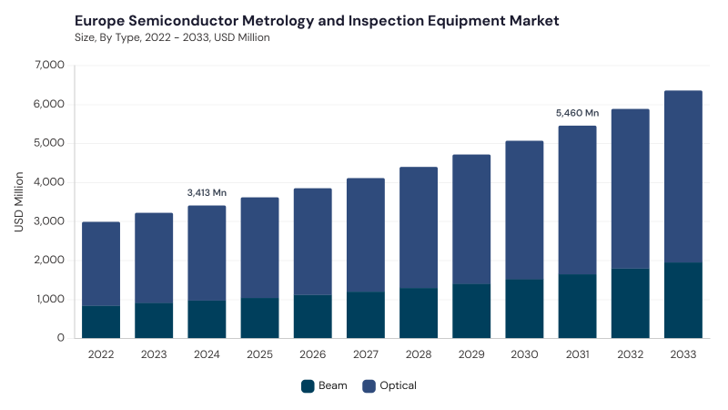
Based on Type, the market is segmented into Optical and Beam. The Optical market dominated the Europe Semiconductor Metrology and Inspection Equipment Market by Type in 2025, and would continue to be a dominant market till 2033; thereby, achieving a market value of USD 3.8 billion by 2031, growing at a CAGR of 7 % during the forecast period. The Beam market is expected to witness a CAGR of 8.3% during (2026 - 2033).
Optical leads due to its rapid, non-contact inspection capability, strong fit with inline wafer monitoring, and widespread use across high-volume semiconductor production environments. These systems support surface defect detection, overlay control, pattern inspection, thin film measurement, and production quality monitoring with strong throughput efficiency. Demand is reinforced by Europe’s focus on precision manufacturing, advanced process control, and expanding semiconductor fabrication investments. Beam-based systems remain important for ultra-high-resolution inspection, critical dimension analysis, EUV process monitoring, mask review, and nanoscale defect characterization where optical systems require complementary support.
Based on Dimension, the market is segmented into 2D Metrology/Inspection, 3D Metrology/Inspection, and Hybrid 2D/3D Systems. The 2D Metrology/Inspection market dominated the Europe Semiconductor Metrology and Inspection Equipment Market by Dimension in 2025, and would continue to be a dominant market till 2033; thereby, achieving a market value of USD 2.5 billion by 2031, growing at a CAGR of 7 % during the forecast period. The 3D Metrology/Inspection market is expected to witness a CAGR of 7.8% during (2026 - 2033). The Hybrid 2D/3D Systems market is expected to witness a CAGR of 7.8% during (2026 - 2033).
2D Metrology/Inspection leads due to its continued importance in routine wafer measurement, linewidth control, overlay verification, planar defect detection, and production quality assurance. These systems remain widely used because they provide reliable, fast, and cost-effective inspection support across mature and advanced manufacturing flows. 3D Metrology/Inspection is gaining traction as European chipmakers expand advanced packaging, MEMS, chiplets, heterogeneous integration, and complex device architectures. Hybrid 2D/3D Systems are gradually expanding as manufacturers seek integrated inspection platforms that combine surface and structural analysis to improve process flexibility and yield management.
Based on End-User, the market is segmented into Foundries, Integrated Device Manufacturing Firms, Outsourced Semiconductor Assembly and Test Companies, and Other End-User. The Foundries market dominated the Europe Semiconductor Metrology and Inspection Equipment Market by End-User in 2025, and would continue to be a dominant market till 2033; thereby, achieving a market value of USD 2.4 billion by 2031, growing at a CAGR of 6.8 % during the forecast period. The Integrated Device Manufacturing Firms market is expected to witness a CAGR of 7.6% during (2026 - 2033). Additionally, The Outsourced Semiconductor Assembly and Test Companies market is expected to witness highest CAGR of 8.2% during (2026 - 2033).
Foundries lead due to their strong need for precise process control, wafer-level inspection, defect monitoring, yield improvement, and high-volume manufacturing consistency. These facilities use advanced metrology tools to support lithography, etching, CMP, deposition, and inline process feedback across complex production nodes. Integrated Device Manufacturing Firms deploy inspection equipment across wafer fabrication, process development, assembly, packaging, and final product verification. Outsourced Semiconductor Assembly and Test Companies and Other End-User areas add demand through package inspection, wire bond verification, solder joint analysis, MEMS development, compound semiconductor research, materials characterization, and pilot-line innovation.
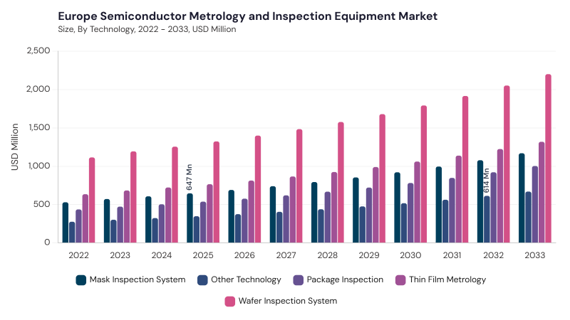
Based on Technology, the market is segmented into Wafer Inspection System, Thin Film Metrology, Mask Inspection System, Package Inspection, and Other Technology. Wafer Inspection System leads due to its central role in early defect detection, wafer quality control, process monitoring, and yield protection throughout semiconductor fabrication. These systems help identify contamination, pattern errors, line edge issues, and process-induced anomalies before they affect downstream manufacturing.
Thin Film Metrology supports accurate measurement of film thickness, refractive properties, layer uniformity, and deposited material performance across critical process steps. Mask Inspection System, Package Inspection, and Other Technology areas add demand through EUV photomask verification, package reliability testing, X-ray inspection, acoustic microscopy, wavefront phase imaging, electron-beam metrology, and specialized next-generation process control.
Free Valuable Insights: The Worldwide Semiconductor Metrology and Inspection Equipment Market is projected to reach USD 26.8 Billion billion by 2033, at a CAGR of 7.6%
Based on Country, the market is segmented into Germany, UK, France, Russia, Spain, Italy, and Rest of Europe. The Germany market dominated the Europe Semiconductor Metrology and Inspection Equipment Market by Country in 2025, and would continue to be a dominant market till 2033; thereby, achieving a market value of USD 1.5 billion by 2031, growing at a CAGR of 6.3 % during the forecast period. The UK market is expected to witness a CAGR of 6.3% during (2026 - 2033). Additionally, The France market is expected to witness a CAGR of 8.3% during (2026 - 2033).
Germany leads due to its precision manufacturing base, semiconductor equipment ecosystem, automotive chip demand, advanced packaging activity, and strong adoption of AI-enabled metrology tools. The UK supports market growth through semiconductor innovation programs, traceable measurement systems, AI-driven inspection development, and advanced chip architecture research. France contributes through 3D IC inspection, virtual metrology, localized R&D, sensor fusion, and Industry 4.0-focused semiconductor manufacturing. Russia, Spain, and Italy add demand through hybrid metrology adoption, domestic production efforts, modular inspection platforms, photonics-based measurement, and localized service support, while Rest of Europe benefits from smart manufacturing, regional semiconductor resilience, and advanced wafer inspection adoption.
By Type
By Dimension
By End-User
By Technology
By Country
Set to reach $5.5 Billion by 2031, growing at 7.4% CAGR during 2026-2033.
Germany leads with $1.5 billion by 2031, growing at a CAGR of 6.3% during the forecast period.
Rising demand for optical equipment, reaching $3.8 billion by 2031, with a CAGR of 7% during the forecast period.
The 2D metrology/inspection segment will reach $2.5 billion by 2031, growing at a CAGR of 7% during the forecast period.
The France market is expected to witness a CAGR of 8.3% during 2026-2033.
The UK market is expected to witness a CAGR of 6.3% during 2026-2033.
Our team of dedicated experts can provide you with attractive expansion opportunities for your business.




 Unique Offerings