“Global Gallium Nitride (GaN) Semiconductor Devices Market to reach a market value of USD 16.78 Billion by 2032 growing at a CAGR of 24.4%”
The Global Gallium Nitride (GaN) Semiconductor Devices Market size is expected to reach $16.78 billion by 2032, rising at a market growth of 24.4% CAGR during the forecast period.
The North America segment recorded 45% revenue share in the market in 2024. The strong presence of prominent semiconductor manufacturers and extensive investments in research and development are the primary reasons for the region's dominance. The United States, in particular, has been at the forefront of GaN technology adoption, driven by advancements in telecommunications, defense, and aerospace sectors.
 Semiconductor Devices Market Size - Global Opportunities and Trends Analysis Report 2021-2032")
Unlike traditional silicon-based devices, GaN semiconductors offer superior efficiency, high-frequency handling, and robustness, making them an ideal choice for modern electronic applications. Their efficiency stems from lower power losses even at high voltages and frequencies, which results in reduced energy consumption and enhanced thermal management. Hence, the ongoing trend toward more efficient and resilient electronic devices continues to propel the growth of the market, cementing its position as a key technology for the future.
Additionally, GaN’s unique properties, particularly its high-frequency switching capabilities, make it ideal for wireless power transfer applications. Unlike traditional silicon-based semiconductors, GaN can operate efficiently at higher frequencies, significantly reducing power loss and enhancing the overall charging speed and efficiency. As a result, GaN-powered wireless chargers are faster and more energy-efficient, meeting the increasing consumer demand for quick and hassle-free charging solutions. Therefore, as wireless charging continues to evolve and expand into various applications, GaN’s role as a fundamental technology in the wireless power transfer ecosystem is becoming increasingly prominent, solidifying its importance in the market.
However, Unlike traditional silicon-based devices, GaN devices require specialized and advanced manufacturing processes that increase overall expenses. The production of GaN components involves using expensive substrates like silicon carbide (SiC) or sapphire, as GaN lacks a native substrate that matches its crystal structure. This mismatch often leads to defects, reducing yield and increasing the cost per unit. Additionally, the epitaxial growth process, essential for producing high-quality GaN layers, demands precise control and high-end equipment, further reducing manufacturing costs. In conclusion, this hesitation among manufacturers slows the adoption of GaN technology, limiting its market potential primarily to niche applications where its superior performance justifies the higher cost.
 Semiconductor Devices Market Share 2024")
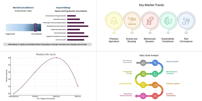
The leading players in the market are competing with diverse innovative offerings to remain competitive in the market. The above illustration shows the percentage of revenue shared by some of the leading companies in the market. The leading players of the market are adopting various strategies in order to cater demand coming from the different industries. The key developmental strategies in the market are Acquisitions, and Partnerships & Collaborations.
Based on product, the market is classified into GaN radio frequency devices, opto-semiconductors, and power semiconductors. The GaN radio frequency devices segment procured 29% revenue share in the market in 2024. The increasing utilization of GaN RF components in applications necessitating high power density, efficiency, and thermal management is the primary factor driving the growth of this segment. These devices are critical in advanced communication systems, including 5G infrastructure, satellite communication, and defense applications.
By wafer size, the market is segmented into 2-inch, 4-inch, 6-inch, and 8-inch. The 6-inch segment garnered 29% revenue share in the market in 2024. The adoption of 6-inch wafers has been accelerating, driven by the increasing demand for higher production efficiency and scalability. As manufacturers strive to reduce costs and increase output, the larger wafer size becomes advantageous, allowing more devices to be fabricated per batch. This is particularly important for power electronics and telecommunications applications, where high-volume production is essential.
 Semiconductor Devices Market Share and Industry Analysis Report 2024")
Based on application, the market is classified into lighting & lasers, power devices, supplies & inverters, and radio frequency (RF). The lighting & lasers segment acquired 24% revenue share in the market in 2024. GaN-based optoelectronic devices, including LEDs and laser diodes, are renowned for their high efficiency, long lifespan, and low power consumption. The rapid adoption of LED technology in residential, commercial, and automotive lighting solutions has been a major growth driver for this segment. The increasing use of GaN lasers in industrial, medical, and consumer electronics applications has also contributed to its substantial market share.
On the basis of component, the market is divided into power IC, transistor, rectifier, diode, and others. The transistor segment attained 23% revenue share in the Gallium Nitride (GaN) semiconductor devices market in 2024. This reflects the growing demand for GaN transistors in various applications such as power electronics, RF devices, and optoelectronics. This segment's expansion is driven by GaN's superior efficiency, higher power density, and ability to operate at higher frequencies compared to traditional semiconductor materials like silicon.
Free Valuable Insights: Global Gallium Nitride (GaN) Semiconductor Devices Market size to reach USD 16.78 Billion by 2032
Region-wise, the market is analyzed across North America, Europe, Asia Pacific, and LAMEA. The Asia Pacific segment witnessed 24% revenue share in the market in 2024. Rapid industrialization and technological advancements in China, Japan, South Korea, and India primarily drive the region's growth. The adoption of GaN-based devices is being expedited by the fact that the Asia Pacific region is a global manufacturing center for telecommunications equipment, automotive components, and consumer electronics.
| Report Attribute | Details |
|---|---|
| Market size value in 2024 | USD 2.96 Billion |
| Market size forecast in 2032 | USD 16.78 Billion |
| Base Year | 2024 |
| Historical Period | 2021 to 2023 |
| Forecast Period | 2025 to 2032 |
| Revenue Growth Rate | CAGR of 24.4% from 2025 to 2032 |
| Number of Pages | 349 |
| Number of Tables | 480 |
| Report coverage | Market Trends, Revenue Estimation and Forecast, Segmentation Analysis, Regional and Country Breakdown, Market Share Analysis, Porter’s 5 Forces Analysis, Company Profiling, Companies Strategic Developments, SWOT Analysis, Winning Imperatives |
| Segments covered | Product, Wafer Size, Application, Component, Region |
| Country scope |
|
| Companies Included | Fujitsu Limited, NXP Semiconductors N.V., Texas Instruments, Inc., Infineon Technologies AG, Qorvo, Inc., Mitsubishi Electric Corporation, Sumitomo Electric Industries, Ltd., STMicroelectronics N.V., NextGen Power Systems, Inc., and Efficient Power Conversion Corporation, Inc. |
By Product
By Wafer Size
By Application
By Component
By Geography
This Market size is expected to reach $16.78 billion by 2032.
Rising Demand for High-Performance Electronics are driving the Market in coming years, however, Substantially High Production Costs restraints the growth of the Market.
Fujitsu Limited, NXP Semiconductors N.V., Texas Instruments, Inc., Infineon Technologies AG, Qorvo, Inc., Mitsubishi Electric Corporation, Sumitomo Electric Industries, Ltd., STMicroelectronics N.V., NextGen Power Systems, Inc., and Efficient Power Conversion Corporation, Inc.
The expected CAGR of this Market is 24.4% from 2023 to 2032.
The Radio Frequency (RF) segment led the maximum revenue in the Market by Application in 2024, thereby, achieving a market value of $5.00 billion by 2032.
The North America region dominated the Devices Market by Region in 2024, thereby, achieving a market value of $7.27 billion by 2032.
Our team of dedicated experts can provide you with attractive expansion opportunities for your business.

 Semiconductor Devices Market")