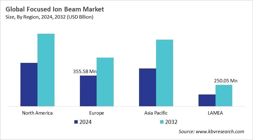
According to a new report, published by KBV research, The Global Focused Ion Beam Market size is expected to reach $2.43 billion by 2032, rising at a market growth of 6.9% CAGR during the forecast period.
Focused ion beam (FIB) systems, which use a high-precision ion beam—usually gallium—from liquid metal sources and imaging capabilities like those of electron microscopes, have changed from simple research tools to advanced tools that are used in many scientific and industrial fields. In the 1970s and 1980s, university labs and national research centers did early studies that led to the development of dual-beam FIB SEM systems that combined milling, deposition, and high-resolution imaging. Thermo Fisher Scientific (via its FEI history), Hitachi High Technologies, JEOL, and TESCAN are among the best OEMs. They all have decades of expertise making electron and ion beam instruments.

The Ga+ Liquid Metal segment is experiencing a CAGR of 6.6 % during the forecast period. This authority may be traced back to its widespread use in modifying semiconductor devices, making nanostructures, and analyzing failures. People like Ga+ liquid metal FIB systems because they can make very high-resolution images. They are utilized a lot in research labs and in industry R&D environments. They are the best choice for applications that need sub-nanometer scale accuracy since they can give accurate beam control and better imaging.
The Electronics & Semiconductor segment led the maximum revenue in the Global Focused Ion Beam Market by Vertical in 2024, thereby, achieving a market value of $1.2 billion by 2032. A lot of semiconductor production operations, such as circuit editing, failure analysis, and mask repair, require FIB systems, which is why they are so popular. As integrated circuits get more complicated and electronic parts get smaller, the requirement for accurate material modification and defect analysis has grown. This has led to an increase in the need for FIB solutions in this field.
The Failure Analysis segment is growing at a CAGR of 6 % during the forecast period. Focused ion beam systems are very important for finding faults and figuring out why microelectronic devices fail. Engineers can do thorough inspections and make corrections quickly since they can mill and image particular areas of concern with great accuracy. This application is very important in making semiconductors and making sure they are of high quality, where reducing flaws is the most important thing.
Full Report: https://www.kbvresearch.com/focused-ion-beam-market/
The North America region dominated the Global Focused Ion Beam Market by Region in 2024, and would continue to be a dominant market till 2032; thereby, achieving a market value of $845 Million by 2032. The Asia Pacific region is anticipated to grow at a CAGR of 7.4% during (2025 - 2032). Additionally, The Europe region would witness a CAGR of 6.1% during (2025 - 2032).
By Wafer Size
By Application
By Substrate Technology
By End Use Industry
By Geography
 Unique Offerings