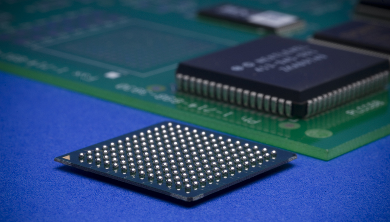
Flip-chip describes the technology of connecting the die electrically to the package carrier. The package carrier can either be a lead frame or substrate or then supply the connection from the die to the external part of the package.
In the typical packaging process, the interconnection between the carrier and the die is set up by using a wire. The die is then connected to the carrier, and then a wire is bonded first to the die, then looped and bonded to the carrier. The length of wires is typically 1-5mm.
On the other hand, in flip-chip technology, the interconnection between the die and the carrier is set up through a bump which is located on the die surface. The height of the bump is typically 0.06 to 0.1mm.
In the advances of the packaging of electronics, the goal is to increase the density of packaging, lower cost, and improve performance. And this is done while increasing the reliability of the circuits. A chip of semiconductor is set up face down into the circuit board is perfect for size considerations as there is no extra space wanted for contacting on the sides of the component. And the process is basically done using flip chip technology.
Flip-chip is not a new technology. To provide links between bonding pads of the chips and the metallization on the substrate, flip-chip technology has been developed by IBM Corporation since 1960s. It is the first proposed method called the Controlled Collapse Chip Connection (C4) to displace wire bolding, expanded IO density, and cost reduction.
The C4 process begins with sticking under bump metallurgy (UBM) on the bonding pads of chips to provide a good union between the bonding pads and the bumps. Generally, UBM consists of three layers of barrier and/or adhesion layer, wetting layer, an oxidation barrier layer.
The performance in high-frequency applications of flip-flop technology is superior to other methods. This is achieved because flip flop technology minimized the length of the connection path. Moreover, due to the reduced number of connections, the reliability is better than with packaged components. There is only one level of joining connection between the chip and the circuit board in flip-chip technology.
Smaller size: Due to the small IC footprint which is only about 5% of that of packaged IC. This helps in reducing height and weight.
Reduced Cost: Flip-chip technology offers cost reductions in batch bumping processes and under fill process.
Increased Reliability: Flip flop technology can decrease the number of connections per pin from three to one. Additionally, Epoxy under fill in big chips ensures and improves high reliability.
Improved Performance: Short and small interconnect provides low capacitance, inductance, and resistance, small electric delays, and better high-frequency features, etc.
Increased functionality: The usage of flip flop provides an increment in the number of I/O. Unlike in wire bonding, I/O is not limited to the perimeter of the chip. 400 pads can easily be handled by a flip-chip.
Flip-chip will continue to exist as growing technology in the coming future. It will continue to redefine the continuum of product and process solutions for the interconnection of the die to the exterior world.
Though flip-chip technology has been there for many years, it is still widely used today also. There are many technical variations in this technology with different levels of maturity. Improvements are underway that will apply a backside lamination coating (BSL). This will protect the less active side of the die against mechanical impact and light. Moreover, BSL will improve the readability of the laser marking under bright field illumination.
Comparatively, flip-chip technology is cheaper than wire bonding. It is since bonding of all connections in the flip-chip system takes place simultaneously while one bond is made at a time in wire bonding technology.
Today flip-chip technologies are widespread in watches, mobile phones disk drivers, hearing aids, LCDs, automotive engine controllers, portable communications as well as mainframe computers.
Low cost, performance, and other beneficial factors have become the key drivers for the adoption of flip-chip technologies.
The flip-chip market is in a growing phase and we hope it will flourish more in the future. Today flip-chips remain a novel development with a big scope for further developments. Developments in the technology of semiconductors have created flip-chips with transistor counts and functions that were difficult to imagine a few years ago. Today flip-chips are available in various ranges of pitches to meet the need and demands of specific applications.
Various factors from Silicon industry has been the driver for the demand of flip-chip technology. Flip-chip technology has travelled a long way. From the three-bump chip to 10,000-bump chip and could be a 50,000-bump chip in the years to come. Flip-chip is facing severe competition due to technological advancements in many contemporary technologies.
Flip-chip technology continues to evolve and play a significant role in various domains. It can adapt to the current challenges due to recent developments in bumping solutions that serve the most advanced packaging technologies. It continues to hold significant advantages over the other microelectronic packaging.
Flip-chip has been developed by electroplating or pastes printing processes. Recent advances in the low-cost package and high-density substrates have promoted the use of flip-chip applications. Flip-chip technologies have been extensively used for the processors of smart phones, tablet games, personal computers, and servers, etc. The Global Flip-chip Market size is expected to rise at a market growth of 8.2% CAGR during the forecast period.